Graphene-based adaptive camouflage : Radar-absorbing materials are used in stealth technologies for concealment of an object from radar detection. Resistive and/or magnetic composite materials are used to reduce the backscattered microwave signals. Inability to control electrical properties of these materials, however, hinders the realization of active camouflage systems. Our group is working on new approaches for adaptive camaoflage systems using large-area graphene electrodes. We developed active surfaces that enable electrical control of reflection, transmission and absorption of microwaves. Instead of tuning bulk material property, our strategy relies on electrostatic tuning of the charge density on an atomically thin electrode, which operates as a tunable metal in microwave frequencies. Notably, we report large-area adaptive radar-absorbing surfaces with tunable reflection suppression ratio up to 50 dB with operation voltages <5 V. Using the developed surfaces, we demonstrate various device architectures including pixelated and curved surfaces. Our results provide a significant step in realization of active camouflage systems in microwave frequencies.
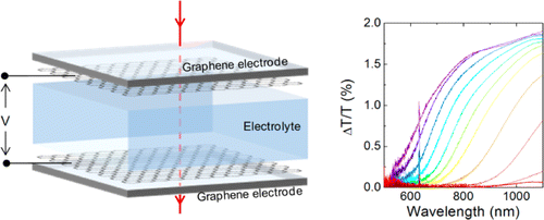
Graphene based electrochromic devices: Graphene emerges as a viable material for optoelectronics because of its broad optical response and gate-tunable properties. For practical applications, however, single layer graphene has performance limits due to its small optical absorption defined by fundamental constants. We are working on a new class of flexible electrochromic devices using multilayer graphene (MLG) which simultaneously offers all key requirements for practical applications; high-contrast optical modulation over a broad spectrum, good electrical conductivity and mechanical flexibility. Our method relies on electro-modulation of interband transition of MLG via intercalation of ions into the graphene layers. The electrical and optical characterizations reveal the key features of the intercalation process which yields broadband optical modulation up to 55 per cent in the visible and near-infrared. We illustrate the promises of the method by fabricating reflective/transmissive electrochromic devices and multi-pixel display devices. Simplicity of the device architecture and its compatibility with the roll-to-roll fabrication processes, would find wide range of applications including smart windows and display devices. We anticipate that this work provides a significant step in realization of graphene based optoelectronics.
Graphene-based photonics: Optical modulators are commonly used in communication and information technology to control intensity, phase, or polarization of light. Electro-optic, electroabsorption, and acousto-optic modulators based on semiconductors and compound semiconductors have been used to control the intensity of light. Because of gate tunable optical properties, graphene introduces new potentials for optical modulators. The operation wavelength of graphene-based modulators, however, is limited to infrared wavelengths due to inefficient gating schemes. Here, we report a broadband optical modulator based on graphene supercapacitors formed by graphene electrodes and electrolyte medium. The transparent supercapacitor structure allows us to modulate optical transmission over a broad range of wavelengths from 450 nm to 2 μm under ambient conditions. We also provide various device geometries including multilayer graphene electrodes and reflection type device geometries that provide modulation of 35%. The graphene supercapacitor structure together with the high-modulation efficiency can enable various active devices ranging from plasmonics to optoelectronics.
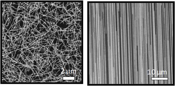 Synthesis of carbon nanotube arrays: The unique electronic properties of single-walled carbon nanotubes (SWNTs) make them promising candidates for next generation electronics,particularly in systems that demand high frequency (e.g., radio frequency, RF) operation. Transistors that incorporate perfectly aligned, parallelarrays of SWNTs avoid the practical limitations of devices that use individual tubes, and they also enable comprehensive experimental and theoretical evaluation of the intrinsic properties. Thus, devices consisting of arrays represent a practical route to use of SWNTs for RFdevices and circuits. The results reveal many aspects of device operation in such array layouts, including full compatibilitywith conventional small signal models of RF response. Submicrometer channel length devices show unity current gain ) and unity powergain frequencies (fmax) as high as ∼5 and ∼9 GHz, respectively, with measured scattering parameters (S-parameters) that agree quantitativelywith calculation.
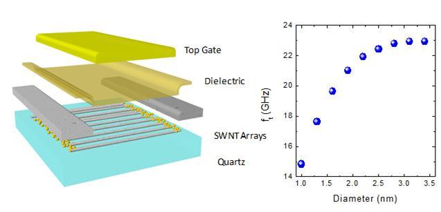 Modeling of carbon nanotube transistors:We are studying high frequency performance limits of single-walled carbon nanotube (SWNT) transistors in the diffusive transport regime limited by the acoustic phonon scattering. The relativistic band structure of single-walled carbon nanotubes combined with the acoustic phonon scattering provides an analytical model for the charge transport of the radio frequency transistors. We were able to obtain the intrinsic high frequency performance such as the cut-off frequency and the linearity of SWNTs transistors. Our model includes transistors based on arrays of SWNTs. The effect of electrostatic screening in a dense array of SWNT on the cut-off frequency can be studied.
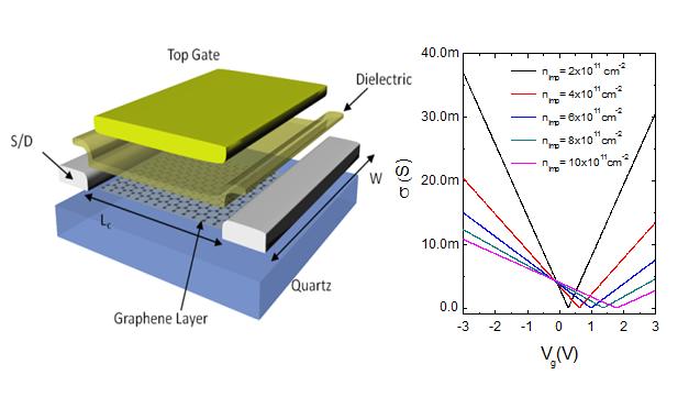
GrapheneRF: Extremely high field effect mobility together with the high surface coverage makes graphene a promising material for high frequency electronics application. We investigate the intrinsic high frequency performance limit of graphene field effect transistors using a self consistent transport model. The self-consistent transport model is based on a nonuniversal diffusive transport that is governed by the charged impurity scattering owing to the presence of the charged impurities on the substrate. The output and transfer characteristics of graphene transistors together with their high frequency performance are characterized as a function of impurity concentration and dielectric constant of the gate insulator.
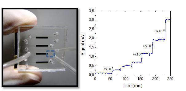
Dynamic microfluidic sensors: A new type of differential surface plasmon (SPR) sensor integrated with a microfluidic system is presented. The working principle of the microfluidic device is based on hydrodynamic modulation of two laminar streams inside a microchannel to provide periodic changes of the environment on the SPR sensor. The modulated reflectance is then demodulated using a lock-in amplifier. The presented sensor provides sensitivities of index of refraction about 4×10⁻⁸ RIU together with a 4 orders of magnitude dynamic range. This method demonstrates a sensitive detection scheme which could be used for label-free detection.


